- 您现在的位置:买卖IC网 > Sheet目录2006 > LTC2755AIUP-16#PBF (Linear Technology)IC DAC 16BIT CUR OUT 64-QFN
LTC2755
4
2755f
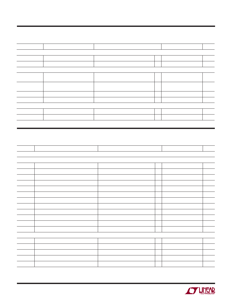
SYMBOL
PARAMETER
CONDITIONS
MIN
TYP
MAX
UNITS
Power Supply
VDD
Supply Voltage
●
2.7
5.5
V
IDD
Supply Current, VDD
Digital Inputs = 0V or VDD
●
0.5
1
μA
Digital Inputs
VIH
Digital Input High Voltage
3.3V ≤ VDD ≤ 5.5V
2.7V ≤ VDD < 3.3V
●
2.4
2
V
VIL
Digital Input Low Voltage
4.5V < VDD ≤ 5.5V
2.7V ≤ VDD ≤ 4.5V
●
0.8
0.6
V
IIN
Digital Input Current
VIN = GND to VDD
●
±1
μA
CIN
Digital Input Capacitance
VIN = 0V (Note 11)
●
6pF
Digital Outputs
VOH
IOH = 200μA
2.7V ≤ VDD ≤ 5.5V
●
VDD – 0.4
V
VOL
IOL = 200μA
2.7V ≤ VDD ≤ 5.5V
●
0.4
V
TIMING CHARACTERISTICS The ● denotes specications that apply over the full operating temperature range,
otherwise specications are at TA = 25°C.
SYMBOL
PARAMETER
CONDITIONS
MIN
TYP
MAX
UNITS
VDD = 4.5V to 5.5V
Write and Update Timing
t1
I/O Valid to WR Rising Edge Set-Up
●
7ns
t2
I/O Valid to WR Rising Edge Hold
●
7ns
t3
WR Pulse Width Low
●
15
ns
t4
UPD Pulse Width High
●
15
ns
t5
UPD Falling Edge to WR Falling Edge
No Data Shoot-Through
●
0ns
t6
WR Rising Edge to UPD Rising Edge
(Note 11)
●
0ns
t7
D/S Valid to WR Falling Edge Set-Up Time
●
7ns
t8
WR Rising Edge to D/S Valid Hold Time
●
7ns
t9
A2-A0 Valid to WR Falling Edge Setup Time
●
5ns
t10
WR Rising Edge to A2-A0 Valid Hold Time
●
0ns
t11
A2-A0 Valid to UPD Rising Edge Setup Time
●
9ns
t12
UPD Falling Edge to A2-A0 Valid Hold Time
●
7ns
Readback Timing
t13
WR Rising Edge to READ Rising Edge
●
7ns
t14
READ Falling Edge to WR Falling Edge
(Note 11)
●
20
ns
t15
READ Rising Edge to I/O Propagation Delay
CL = 10pF
●
40
ns
t26
A2-A0 Valid to READ Rising Edge Setup Time
●
20
ns
t27
READ Falling to A2-A0 Valid Hold Time
(Note 11)
●
0ns
ELECTRICAL CHARACTERISTICS V
DD = 5V, VREF = 5V unless otherwise specied. The ● denotes the
specications which apply over the full operating temperature range, otherwise specications are at TA = 25°C.
发布紧急采购,3分钟左右您将得到回复。
相关PDF资料
LTC2757ACLX#PBF
IC DAC 18BIT PAR 48LQFP
LTC2758AILX#PBF
IC DAC 18BIT SPI/SRL 48-LQFP
LTC2844IG#TRPBF
IC TXRX 3.3V MULTIPROTCOL 28SSOP
LTC2852MPS#PBF
IC TXRX RS485 20MBPS 14-SOIC
LTC486ISW#TRPBF
IC DVR RS485 LOW PWR QUAD 16SOIC
LTC490IS8#TRPBF
IC TXRX RS485 LOW POWER 8-SOIC
LTC491IS#TRPBF
IC TXRX RS485 LOW POWER 14-SOIC
LTC6900IS5#TR
IC OSC SILICON 20MHZ TSOT23-5
相关代理商/技术参数
LTC2755AIUP-16#TRPBF
功能描述:IC DAC 16BIT CUR OUT 64-QFN RoHS:是 类别:集成电路 (IC) >> 数据采集 - 数模转换器 系列:SoftSpan™ 产品培训模块:Data Converter Fundamentals
DAC Architectures 标准包装:750 系列:- 设置时间:7µs 位数:16 数据接口:并联 转换器数目:1 电压电源:双 ± 功率耗散(最大):100mW 工作温度:0°C ~ 70°C 安装类型:表面贴装 封装/外壳:28-LCC(J 形引线) 供应商设备封装:28-PLCC(11.51x11.51) 包装:带卷 (TR) 输出数目和类型:1 电压,单极;1 电压,双极 采样率(每秒):143k
LTC2755BCUP-16#PBF
功能描述:IC DAC 16BIT CUR OUT 64-QFN RoHS:是 类别:集成电路 (IC) >> 数据采集 - 数模转换器 系列:SoftSpan™ 标准包装:1 系列:- 设置时间:4.5µs 位数:12 数据接口:串行,SPI? 转换器数目:1 电压电源:单电源 功率耗散(最大):- 工作温度:-40°C ~ 125°C 安装类型:表面贴装 封装/外壳:8-SOIC(0.154",3.90mm 宽) 供应商设备封装:8-SOICN 包装:剪切带 (CT) 输出数目和类型:1 电压,单极;1 电压,双极 采样率(每秒):* 其它名称:MCP4921T-E/SNCTMCP4921T-E/SNRCTMCP4921T-E/SNRCT-ND
LTC2755BCUP-16#TRPBF
功能描述:IC DAC 16BIT CUR OUT 64-QFN RoHS:是 类别:集成电路 (IC) >> 数据采集 - 数模转换器 系列:SoftSpan™ 产品培训模块:Data Converter Fundamentals
DAC Architectures 标准包装:750 系列:- 设置时间:7µs 位数:16 数据接口:并联 转换器数目:1 电压电源:双 ± 功率耗散(最大):100mW 工作温度:0°C ~ 70°C 安装类型:表面贴装 封装/外壳:28-LCC(J 形引线) 供应商设备封装:28-PLCC(11.51x11.51) 包装:带卷 (TR) 输出数目和类型:1 电压,单极;1 电压,双极 采样率(每秒):143k
LTC2755BIUP-16#PBF
功能描述:IC DAC 16BIT CUR OUT 64-QFN RoHS:是 类别:集成电路 (IC) >> 数据采集 - 数模转换器 系列:SoftSpan™ 产品培训模块:Data Converter Fundamentals
DAC Architectures 标准包装:750 系列:- 设置时间:7µs 位数:16 数据接口:并联 转换器数目:1 电压电源:双 ± 功率耗散(最大):100mW 工作温度:0°C ~ 70°C 安装类型:表面贴装 封装/外壳:28-LCC(J 形引线) 供应商设备封装:28-PLCC(11.51x11.51) 包装:带卷 (TR) 输出数目和类型:1 电压,单极;1 电压,双极 采样率(每秒):143k
LTC2755BIUP-16#TRPBF
功能描述:IC DAC 16BIT CUR OUT 64-QFN RoHS:是 类别:集成电路 (IC) >> 数据采集 - 数模转换器 系列:SoftSpan™ 产品培训模块:Data Converter Fundamentals
DAC Architectures 标准包装:750 系列:- 设置时间:7µs 位数:16 数据接口:并联 转换器数目:1 电压电源:双 ± 功率耗散(最大):100mW 工作温度:0°C ~ 70°C 安装类型:表面贴装 封装/外壳:28-LCC(J 形引线) 供应商设备封装:28-PLCC(11.51x11.51) 包装:带卷 (TR) 输出数目和类型:1 电压,单极;1 电压,双极 采样率(每秒):143k
LTC2755CUP-12#PBF
功能描述:IC DAC 12BIT CUR OUT 64-QFN RoHS:是 类别:集成电路 (IC) >> 数据采集 - 数模转换器 系列:SoftSpan™ 产品培训模块:Data Converter Fundamentals
DAC Architectures 标准包装:750 系列:- 设置时间:7µs 位数:16 数据接口:并联 转换器数目:1 电压电源:双 ± 功率耗散(最大):100mW 工作温度:0°C ~ 70°C 安装类型:表面贴装 封装/外壳:28-LCC(J 形引线) 供应商设备封装:28-PLCC(11.51x11.51) 包装:带卷 (TR) 输出数目和类型:1 电压,单极;1 电压,双极 采样率(每秒):143k
LTC2755CUP-12#TRPBF
功能描述:IC DAC 12BIT CUR OUT 64-QFN RoHS:是 类别:集成电路 (IC) >> 数据采集 - 数模转换器 系列:SoftSpan™ 标准包装:47 系列:- 设置时间:2µs 位数:14 数据接口:并联 转换器数目:1 电压电源:单电源 功率耗散(最大):55µW 工作温度:-40°C ~ 85°C 安装类型:表面贴装 封装/外壳:28-SSOP(0.209",5.30mm 宽) 供应商设备封装:28-SSOP 包装:管件 输出数目和类型:1 电流,单极;1 电流,双极 采样率(每秒):*
LTC2755CUP-14#PBF
功能描述:IC DAC 14BIT CUR OUT 64-QFN RoHS:是 类别:集成电路 (IC) >> 数据采集 - 数模转换器 系列:SoftSpan™ 产品培训模块:Data Converter Fundamentals
DAC Architectures 标准包装:750 系列:- 设置时间:7µs 位数:16 数据接口:并联 转换器数目:1 电压电源:双 ± 功率耗散(最大):100mW 工作温度:0°C ~ 70°C 安装类型:表面贴装 封装/外壳:28-LCC(J 形引线) 供应商设备封装:28-PLCC(11.51x11.51) 包装:带卷 (TR) 输出数目和类型:1 电压,单极;1 电压,双极 采样率(每秒):143k